

The Silicon Power Parity: How Intel 18A and TSMC N2 are Redefining the Economics and Physics of AI Compute

The global semiconductor industry has entered a critical transition phase in the 2nm-class node generation. As of early 2026, supply chain analytics confirm that Intel’s 18A process node has successfully navigated the complexities of high-volume manufacturing, achieving functional yields in the 65% to 75% range. This milestone effectively closes the historical yield gap, placing Intel in direct competition with Taiwan Semiconductor Manufacturing Company (TSMC), whose N2 process is currently maintaining highly stable yields of 65% to 75%. Concurrently, Samsung Foundry’s SF2 node has recovered its footing, pushing yields into the 50% to 70% range.
With manufacturing parity largely achieved at the leading edge, the market response has been pragmatic. Major hyperscalers are actively pursuing dual-sourcing strategies to mitigate supply chain risks: Microsoft is leveraging 18A for its custom Maia AI accelerators, and Amazon AWS is utilizing it for its Trainium architecture. Domestically, the U.S. Department of Defense has fortified Intel’s momentum with a $3 billion Secure Enclave contract.
However, beneath the yield percentages lies a deeper narrative: a divergence in the architectural philosophy of how to sustain the exponential growth of artificial intelligence.
The Architectural Divergence: Density vs. Power Delivery
The competition between TSMC’s N2 and Intel’s 18A is no longer a simple race for transistor shrinkage; it is a debate over how to balance the multifaceted bottlenecks of modern compute. While logic density remains crucial, the ultimate limits of AI hardware are now dictated by a complex synthesis of raw density, power delivery, advanced packaging, and software ecosystems.
The Illusion of Pure Density and the “IR Drop” Crisis
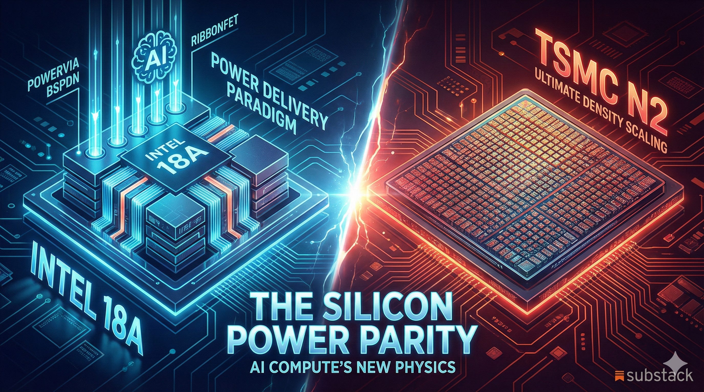
TSMC’s N2 represents the current pinnacle of traditional dimensional scaling, achieving a high-density (HD) standard-cell transistor density of approximately 313 MTr/mm² (million transistors per square millimeter). Intel’s 18A yields roughly 238 MTr/mm².
On paper, TSMC retains a 30% density advantage. Yet, in the context of massive AI accelerators, raw logic density can be a deceptive metric. A modern AI GPU fails not from a lack of logic gates, but because those gates cannot be fed with data and power simultaneously without severe electrical interference and thermal throttling.
The Bottleneck: TSMC’s baseline N2 utilizes a refined Nanosheet Gate-All-Around (GAA) structure but relies on a traditional front-side power delivery network. Both power and signal interconnects must fight for space in the same microscopic metal routing stack on top of the silicon wafer.
The Result: When thousands of AI chips draw immense current spikes, the power traveling through 15+ highly resistive metal layers causes a proportional voltage sag (V=IR), known as the “IR drop.” To compensate, designers must over-provision input voltage, burning excess power as heat and forcing the processor to throttle its clock speeds.
Intel’s Structural Pivot: PowerVia and RibbonFET
Intel’s 18A is a calculated architectural gamble that tackles the IR drop directly, trading some 2D density for supreme 3D power efficiency.
Backside Power Delivery (PowerVia): Intel relocates the entire power delivery network to the backside of the silicon substrate using nano-scale through-silicon vias (nano-TSVs). This decouples power integrity from signal integrity. Independent research indicates that while front-side power delivery through a 15-via chain exhibits ~560 ohms of resistance, a backside nano-via slashes that to roughly 50 ohms—reducing dynamic power drop by up to 75%.
Signal Routing & SRAM: With the front side freed from power routing, 100% of those metal layers are dedicated to signal routing. Furthermore, PowerVia allows the physical footprint of memory arrays to be optimized purely for density, bringing Intel’s 18A SRAM bit cell density (0.023 µm² for high-performance) strictly on par with TSMC’s N2.
RibbonFET: Intel’s 18A utilizes a 4-ribbon stack GAA design (compared to TSMC’s 3-sheet Nanosheet). This gives each individual transistor a larger effective channel width, resulting in higher drive current and more “horsepower per transistor.”
The Broader Battlefield: Ecosystems, Packaging, and Geopolitics
While Intel holds an early architectural advantage in backside power delivery, analyzing this competition solely through the lens of the silicon wafer ignores the broader realities of the semiconductor market in 2026.
1. The Advanced Packaging and Software Moat
AI compute is not just about the die; it is about how multiple dies are stitched together. TSMC’s CoWoS (Chip-on-Wafer-on-Substrate) advanced packaging technology remains the undisputed industry standard, deeply integrated with Nvidia’s dominant CUDA software ecosystem. Even if Intel 18A offers superior power efficiency at the transistor level, Intel Foundry must prove that its EMIB and Foveros packaging solutions can match TSMC’s volume and reliability to truly win over top-tier AI accelerator designs.
2. Geopolitics and Supply Chain Resilience
The shift toward Intel by U.S. hyperscalers and the DoD is not purely technical; it is heavily influenced by geopolitical risk management.
TSMC’s Vulnerability: Despite its operational excellence, TSMC’s deep geographic concentration in Taiwan presents an existential supply chain risk for Western tech giants amid geopolitical tensions.
Intel’s Premium: Intel’s U.S. and European fab expansion, subsidized by the CHIPS Act, offers a geopolitically resilient alternative. Companies like Microsoft and Amazon are willing to invest in dual-sourcing not just for better power delivery, but as an insurance policy.
3. Cost and Capacity Scaling
Achieving 65-75% yield is only the first step. TSMC is historically unparalleled in scaling production capacity quickly while driving down defect densities and wafer costs. Intel must still prove it can translate its 18A technical milestones into economically viable, massive-scale production that matches TSMC’s predictable cadence.
TSMC’s Counter-Offensive and the Future
It would be a critical error to assume TSMC is standing still. Moving into the latter half of 2026 and beyond, TSMC is aggressively rolling out its N2P and highly anticipated A16 nodes, which introduce their own backside power delivery solution: Super Power Rail. This ensures that TSMC will soon combine their established superiority in 2D density scaling with the 3D power efficiencies that currently define Intel’s 18A advantage.
The foundry war has fundamentally shifted. The bottleneck for AI is no longer just how small we can draw a transistor, but the holistic optimization of density, 3D power routing, packaging, and software. The technology gap has largely vanished, leaving the industry in its most balanced and fiercely competitive technical deadlock in a decade.